REV. A
a
AD53522
Information furnished by Analog Devices is believed to be accurate and
reliable. However, no responsibility is assumed by Analog Devices for its
use, nor for any infringements of patents or other rights of third parties that
may result from its use. No license is granted by implication or otherwise
under any patent or patent rights of Analog Devices. Trademarks and
registered trademarks are the property of their respective owners.
One Technology Way, P.O. Box 9106, Norwood, MA 02062-9106, U.S.A.
Tel: 781/329-4700 www.analog.com
Fax: 781/326-8703 © 2003 Analog Devices, Inc. All rights reserved.
High Speed
Dual Pin Electronic
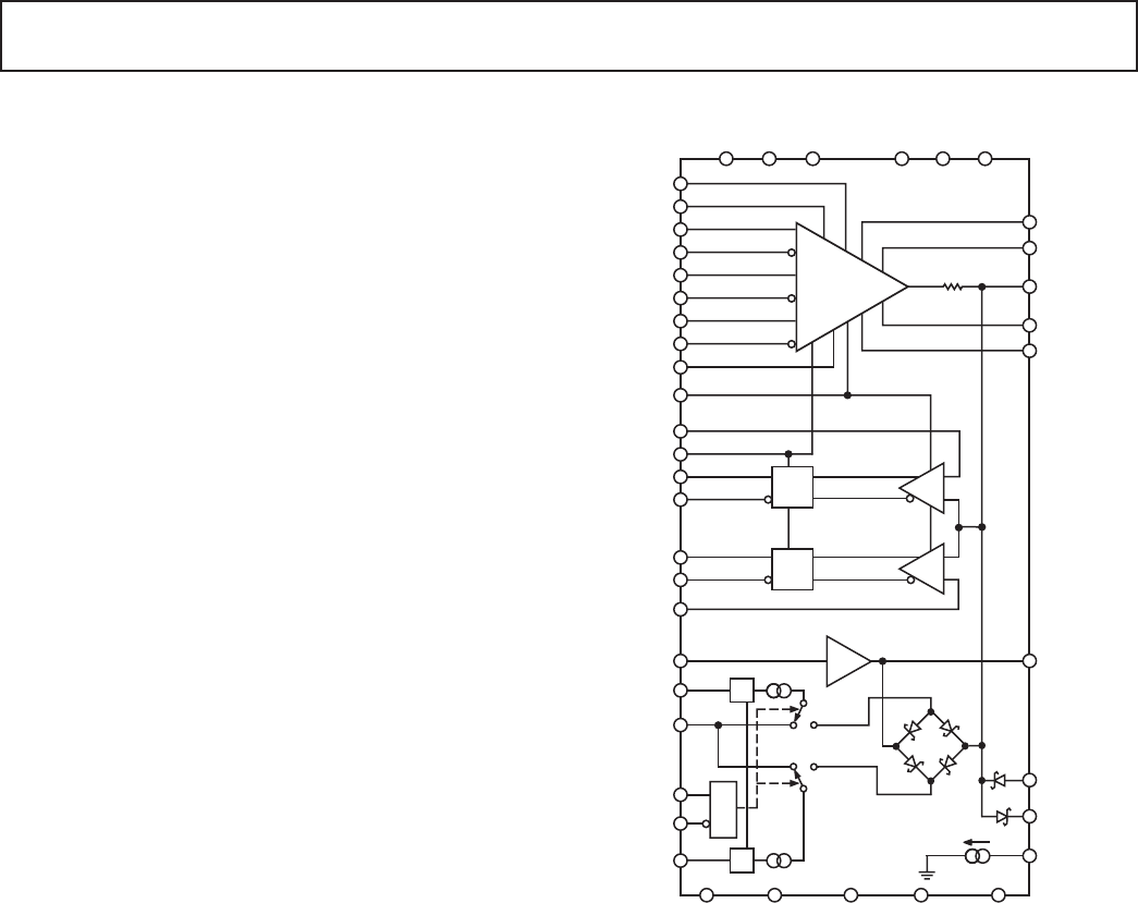
FUNCTIONAL BLOCK DIAGRAM (One-Half)
DRIVER
COMPARATOR
V/I
V/I
ACTIVE LOAD
1.0A/K
V
CC
V
CC
V
CC
V
EE
V
EE
V
EE
AD53522
VHDCPL
OUT
VLDCPL
PWRGND
9
HQGND
VCOM_S
THERM*
+1
VH
VTERM
DATA
IOD
RLD
VL
HCOMP
VCCO
QH
QL
LCOMP
VCOM
IOLC
IOXRTN
INHL
IOHC
VCL
VCH
PROT_HI
PROT_LO
PWRD
GND_ROTDR_GND THERMSTART
*ONLY 1 (ONE) THERM PER DEVICE
INHLB
QLB
QHB
RLDB
IODB
DATAB
FEATURES
1000 MHz Toggle Rate
Driver/Comparator/Active Load and Dynamic Clamp
Included
Inhibit Mode Function
100-Lead LQFP Package with Built-In Heat Sink
Driver
48 Output Resistance
800 ps Tr/Tf for a 3 V Step
Comparator
1.1 ns Propagation Delay at 3 V
Load
40 mA Voltage Programmable Current Range
50 ns Settling Time to 15 mV
APPLICATIONS
Automatic Test Equipment
Semiconductor Test Systems
Board Test Systems
Instrumentation and Characterization Equipment
PRODUCT DESCRIPTION
The AD53522 is a complete, high speed, single-chip solution
that performs the pin electronics functions of driver, comparator,
and active load (DCL) for ATE applications. In addition, the
driver contains a dynamic clamp function and the active load
contains an integrated Schottky diode bridge.
The driver is a proprietary design that features three active states:
Data High mode, Data Low mode, and Term mode, as well as
an Inhibit State. In conjunction with the integrated dynamic
clamp, this facilitates the implementation of a high speed active
termination. The output voltage range is –0.5 V to +6.5 V to
accommodate a wide variety of test devices.
The dual comparator, with an input range equal to the driver
output range, features PECL compatible outputs. Signal tracking
capability is in the range of 3 V/ns.
The active load can be set for up to 40 mA load current. I
OH
, I
OL
,
and the buffered VCOM are independently adjustable. On-board
Schottky diodes provide high speed switching and low capacitance.
Also included is an on-board temperature sensor that gives an
indication of the silicon surface temperature of the DCL. This
information can be used to measure
JC
and
JA
or flag an alarm
if proper cooling is lost. Output from the sensor is a current sink
that is proportional to absolute temperature. The gain is trimmed
to a nominal value of 1.0 µA/K. As an example, the output current
can be sensed by using a 10 kΩ resistor connected from 10 V to
the THERM (I
OUT
) pin. A voltage drop across the resistor will
be developed that equals 10 kΩ ⫻ 1 µA/°K = 10 mV/°K=2.98V
at room temperature.

REV. A
–2–
AD53522–SPECIFICATIONS
DRIVER
1
(T
J
= 85C 5C, +V
S
= +10.5 V 1%, –V
S
= –4.5 V 1%, VCCO = 3.3 V, unless otherwise noted.)
Spec Spec
3
No. Parameter Conditions Min Typ
2
Max Unit Perf
DIFFERENTIAL INPUT CHARACTERISTICS
(DATA to DATAB, IOD to IODB, RLD to RLDB)
1 Voltage Range Note: Inputs are from Same Logic 0 +3.3 V N
Type Family
2 Differential Voltage with Note: AC Tests Performed ± 400 ± 600 ± 1000 mV P
LVPECL Levels
3 Bias Current V
IN
= 1.5 V, 2.5 V –250 +250 µAP
REFERENCE INPUTS
4 Bias Currents Max Value Measured during –50 +50 µAP
Linearity Tests
OUTPUT CHARACTERISTICS
10 Logic High Range Data = H, VH = –0.4 V to +6.5 V, –0.4 +6.5 V P
Vl = –0.5 V (VT = 0 V, VH Meets
Test 20, 21, and 22 Specs)
11 Logic Low Range Data = L, VL = –0.5 V to +6.4 V, –0.5 +6.4 V P
VH = 6.5 V (VT = 0 V, VL Meets
Test 30, 31, and 32 Specs)
12 Amplitude [VH–VL] VL = –0.05 V, VH = +0.05 V, +0.1 +7.0 V P
VT = 0 V and VL = –0.5 V,
VH = +6.5 V, VT = 0 V
ABSOLUTE ACCURACY
20 VH Offset Data = H, VH = 0 V, VL = –0.5 V, –50 +50 mV P
VT = +3 V
21 VH Gain Error Data = H, VH = –0.4 V to +6.5 V, –0.3 +0.3 % of VH P
VL = –0.5 V, VT = +3 V
22 Linearity Error Data = H, VH = –0.4 V to +6.5 V, –5 +5 mV P
VL = –0.5 V, VT = +3 V
30 VL Offset Data = L, VL = 0 V, VH = +6.5 V, –50 +50 mV P
VT = +3 V
31 VL Gain Error Data = L, VL = –0.5 V to +6.4 V, –0.3 +0.3 % of VL P
VH = +6.5 V, VT = +3 V
32 Linearity Error Data = L, VL = –0.5 V to +6.4 V, –5 +5 mV P
VH = +6.5 V, VT = +3 V
33 Offset Temperature Coefficient VL = 0 V, VH = +5 V, VT = 0 V +0.5 mV/°CN
OUTPUT RESISTANCE
40 VH = –0.3 V VL = –0.5 V, VT = 0 V, I
OUT
= +1, +46 +50 Ω N
+30 mA
41 VH = +6.5 V VL = –0.5 V, VT = 0 V, I
OUT
= –1, +46 +50 Ω P
–30 mA
42 VL = –0.5 V VH = +6.5 V, VT = 0 V, I
OUT
= +1, +46 +50 Ω P
+30 mA
43 VL = +6.4 V VH = +6.5 V, VT = 0 V, I
OUT
= –1, +46 +50 Ω N
–30 mA
44 VH = +2.5 V VL = 0 V, VT = 0 V, I
OUT
= –30 mA +47.5 Ω P
(Trim Point)
50 Dynamic Current Limit Cbyp = 39 nF, VH = +6.5 V, +100 mA N
VL = –0.5 V, VT = 0 V
51 Static Current Limit Output to –0.5 V, VH = +6.5 V, –120 –60 mA P
VL = –0.5 V, VT = 0 V, DATA = H
52 Static Current Limit Output to +6.5 V, VH = +6.5 V, +60 +120 mA P
VL = –0.5 V, VT = 0 V, DATA = L

REV. A
–3–
AD53522
DRIVER
1
(continued)
Spec Spec
3
No. Parameter Conditions Min Typ
2
Max Unit Perf
VTERM
60 Voltage Range Term Mode, VTERM = –0.3 V –0.3 +6.3 V P
to +6.3 V, VL = 0 V, VH = +3 V
(VTERM Meets Test 61, 62, and 63 specs)
61 VTERM Offset Term Mode, VTERM = 0 V, –50 +50 mV P
VL = 0 V, VH = +3 V
62 VTERM Gain Error Term Mode, VTERM = –0.3 V –0.3 +0.3 % of V
SET
P
to +6.3 V, VL = 0 V, VH = +3 V
63 VTERM Linearity Error
4
Term Mode, VTERM = –0.3 V –5 +5 mV P
to +6.3 V, VL = 0 V, VH = +3 V
64 Offset Temperature Coefficient VTERM = 0 V, VL = 0 V, VH = +3 V +0.5 mV/°CN
70 Output Resistance DC I
OUT
= +30 mA, –1 mA, +46 +50 Ω
VTERM = –0.3 V, VH = +3 V, VL = 0 V N
I
OUT
= –30 mA, +1 mA,
VTERM =+6.3 V, VH = +3 V, VL = 0 V N
I
OUT
= ± 30 mA, ± 1 mA,
VTERM = +2.5 V, VH = +3 V, VL = 0 V P
72 PSRR, Drive, or Term Mode +V
S
, –V
S
± 1% +17.8 mV/V N
73 Static Current Limit Output to –0.3 V, VTERM = +6.3 V –120 –60 mA P
74 Static Current Limit Output to +6.3 V, VTERM = –0.3 V +60 +120 mA P
DYNAMIC PERFORMANCE, DRIVE (VH and VL)
80 Propagation Delay Time Measured at 50%, VL = 0 V, 1.25 1.4 1.55 ns P
VH = 3 V, into 500 Ω
81 Propagation Delay T.C. Measured at 50%, VL = 0 V, 2 ps/°CN
VH = 3 V, into 500 Ω
82 Delay Matching, Edge-to-Edge Measured at 50%, VL = 0 V, 200 ps P
VH = 3 V, into 500 Ω
RISE AND FALL TIMES
90 200 mV Swing Measured 20%–80%, VL = –0.1 V, 0.25 ns N
VH = +0.1 V, into 50 Ω
91 1 V Swing Measured 20%–80%, VL = 0 V, 0.3 ns N
VH = 1 V, into 50 Ω
92 3 V Swing Measured 10%–90%, VL = 0 V, 0.8 ns N
VH = 3 V, into 50 Ω
93 3 V Swing Measured 10%–90%, VL = 0 V, 0.8 ns N
VH = 3 V, into 500 Ω
93A 3 V Swing Measured 20%–80%, VL = 0 V, 0.450 0.560 0.670 ns P
VH = 3 V, into 500 Ω
94 5 V Swing Measured 10%–90%, VL = 0 V, 1.2 1.5 ns N
VH = 5 V, into 500 Ω
RISE AND FALL TIME TEMPERATURE COEFFICIENT
100 1 V Swing (Per Test 91) ± 2 ps/°CN
101 3 V Swing (Per Test 92) ± 2 ps/°CN
102 5 V Swing (Per Test 94) ± 4 ps/°CN
110 Overshoot and Preshoot VL, VH = –0.1 V, +0.1 V, 0 – 50 0 + 50 % of Step N
Driver Terminated into 50 Ω + mV
VL, VH = 0.0 V, 3 V, –6.0 – 50 +6.0 + 50 % of Step N
Driver Terminated into 50 Ω + mV
SETTLING TIME
120 to 15 mV VL = 0 V, VH = 0.5 V, 50 ns N
Driver Terminated into 50 Ω
121 to 4 mV VL = 0 V, VH = 0.5 V 10 µsN
130 Delay Change vs. Pulse Width VL/VH = 0/3, PW = 2.5 ns/7.5 ns, 25 75 ps N
30 ns/90 ns, DC = 25%
131 Delay Change vs. Duty Cycle VL = 0 V, VH = 3 V, Duty Cycle 25 ps N
(DC) 5% to 95%, T = 40 ns


