International Airport Industrial Park • Mailing Address: PO Box 11400 • Tucson, AZ 85734 • Street Address: 6730 S. Tucson Blvd. • Tucson, AZ 85706
Tel: (520) 746-1111 • Twx: 910-952-1111 • Cable: BBRCORP • Telex: 066-6491 • FAX: (520) 889-1510 • Immediate Product Info: (800) 548-6132
3584
High Voltage, High Speed
OPERATIONAL AMPLIFIER
APPLICATIONS
● PROGRAMABLE POWER SUPPLY
● PIEZO-ELECTRIC TRANSDUCER DRIVER
● ELECTROSTATIC TRANSDUCER DRIVER
● CRT DEFLECTION
FEATURES
● WIDE POWER SUPPLY VOLTAGE:
±70V to ±150V
● GAIN-BANDWIDTH PRODUCT: 50MHz
● SLEW RATE: 150V/
µs
● FET INPUT: I
B
= 20pA max
● THERMAL SHUT-DOWN PROTECTION
● HERMETIC TO-3 PACKAGE, ISOLATED
CASE
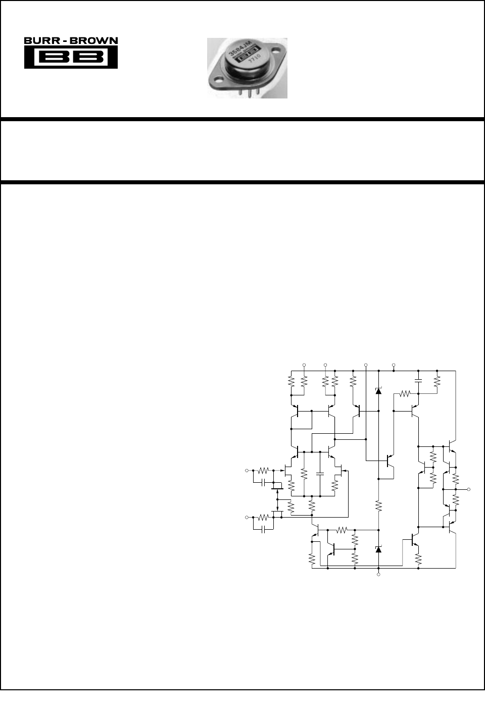
DESCRIPTION
The 3584 is a high voltage, high speed hybrid opera-
tional amplifier designed for a wide variety of
programmable power supply and transducer driver
applications.
The 3584 operates over a wide power supply range
(±70V to ±150V) and provides outputs up to 15mA.
Laser-trimmed FET input circuitry provides low offset
voltage (3mV max) and low input bias current (20pA
max). Thermal shut-down circuitry protects internal
circuitry from excessive power dissipation.
The 3584 provides a gain-bandwidth product of 20MHz
min (50MHz typical). External frequency compensa-
tion (series R/C) allows the user to optimize the
bandwidth and slew rate for a particular application.
Specified temperature range is 0°C to +70°C. The
3584’s hermetic 8-pin TO-3 package is electrically
isolated from all internal circuitry.
Output
1
Offset Trim
3
4 2
V+
8
Compensation
5
–In
6
+In
7
V–
®
©
1978 Burr-Brown Corporation PDS-376B Printed in U.S.A. October, 1993
SBOS131

®
3584
2
3584JM
PARAMETER CONDITIONS MIN TYP MAX UNITS
OFFSET VOLTAGE
Input Offset Voltage ±3mV
vs Temperature Specified Temperature Range ±25 µV/°C
vs Power Supply 20 µV/V
vs Time 50 µV/month
INPUT BIAS CURRENT
(1)
Input Bias Current V
CM
= 0V –20 pA
vs Temperature Doubles Every 10°C
vs Power Supply 0.2 pA/V
Input Offset Current V
CM
= 0V ±20 pA
vs Temperature Doubles Every 10°C
vs Power Supply 0.2 pA/V
NOISE
Voltage, 0.01Hz to 10Hz 5 µVp-p
10Hz to 1kHz 1.7 µVrms
Current, 0.01Hz to 10Hz 0.3 pAp-p
INPUT VOLTAGE RANGE
Maximum Safe Differential Input (V+) + |V–|
Maximum Safe Common-Mode Input V– to V+
Common-Mode Input Range Linear Operation V
S
– 10 V
Common-Mode Rejection 110 dB
INPUT IMPEDANCE
Differential 10
11
||10 Ω || pF
Common-Mode 10
11
Ω || pF
OPEN-LOOP GAIN
Open-Loop Voltage Gain No Load, DC 120 dB
Open-Loop Voltage Gain Rated Load, DC 100 dB
FREQUENCY RESPONSE
Unity-Gain Bandwidth Small-Signal 7 MHz
Gain-Bandwidth Product f = 1kHz, G = 100 20 MHz
Full-Power Bandwidth G = 100 135 kHz
Slew Rate G = 100 150 V/µs
Settling Time: 0.1% G = 100 12 µs
OUTPUT
Voltage Output V
S
- 5 V
Current Output ±15 mA
Short Circuit Current ±25 mA
Load Capacitance (Maximum) 10 nF
POWER SUPPLY
Operating Voltage Range ±70 ±150 V
Quiescent Current I
O
= 0 ±6.5 mA
TEMPERATURE RANGE
Specification 0 +70 °C
Operating –55 +125 °C
Storage –55 +150 °C
The information provided herein is believed to be reliable; however, BURR-BROWN assumes no responsibility for inaccuracies or omissions. BURR-BROWN
assumes no responsibility for the use of this information, and all use of such information shall be entirely at the user’s own risk. Prices and specifications are subject
to change without notice. No patent rights or licenses to any of the circuits described herein are implied or granted to any third party. BURR-BROWN does not
authorize or warrant any BURR-BROWN product for use in life support devices and/or systems.
SPECIFICATIONS
ELECTRICAL
T
CASE
= +25°C, V
S
= ±150V, unless otherwise noted.
NOTE: (1) Inputs may be damaged by input slew rates exceeding 1000V/µs. Inputs can be protected from signals exceeding 1000V/µs by limiting input current to 150mA
with external series resistors (pins 5 and 6).
®
3584
3
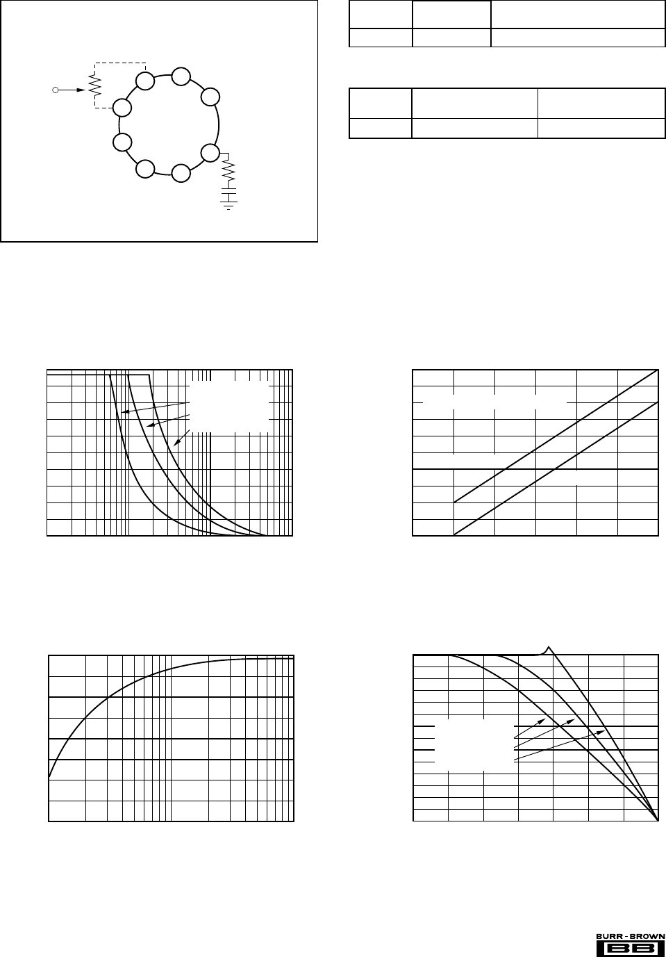
CONNECTION DIAGRAM
ORDERING INFORMATION
TEMPERATURE
MODEL PACKAGE RANGE
3584JM 8-Pin TO-3 0°C to +70°C
TYPICAL PERFORMANCE CURVES
T
CASE
= +25°C, V
S
= ±150V, unless otherwise noted.
Top View
1
2
3
7
8
5
6
+V
CC
–V
CC
Compensation
Output
+In
Offset
Trim
to +V
CC
4
Optional Socket: Burr-Brown Model 0804MC
–In
100kΩ
Offset
Trim
Optional
Offset
Adjust
R
C
C
C
PACKAGE DRAWING
MODEL PACKAGE NUMBER
(1)
3584JM 8-Pin TO-3 030
NOTE: (1) For detailed drawing and dimension table, please see end of data
sheet, or Appendix D of Burr-Brown IC Data Book.
PACKAGE INFORMATION
0
Frequency (Hz)
OUTPUT VOLTAGE vs FREQUENCY
Output Voltage (±Vp-p)
100k 1M10k 10M
150
120
90
60
30
Compensation:
200Ω and 0.1µF
2kΩ and 500pF
20Ω and 50pF
40 50 60 80 90 100
Power Supply (% of max)
70
0.5
SLEW RATE vs SUPPLY VOLTAGE AT FULL LOAD
Normalized Slew Rate
1.0
0.9
0.8
0.7
0.6
25°C to 85°C (Case)
–25°C (Case)
Compensation: 200Ω and 0.01µF
0
External Compensation Impedance (Ω)
SLEW RATE vs COMPENSATION
Slew Rate (V/µs)
2k200 20k
160
120
80
40
Frequency (Hz)
–20
OPEN-LOOP FREQUENCY RESPONSE FULL LOAD
Voltage Gain (dB)
120
100
80
60
40
20
0
1 10k 10M10 100 1k 100k 1M
Compensation:
200Ω and 0.1µF
2kΩ and 500pF
20Ω and 50pF


.jpg "SN3269-SP-B3(H)")